Applications
 Part of the Oxford Instruments Group
Expand
Collapse
Part of the Oxford Instruments Group

By Ben Yager and Abi Graham
Our TeslatronPT system, with its high-magnetic field and cryogenic environment, provides a platform for a variety of applications, including electrical transport measurements (see figure 1), low-dimensional physics and spintronics. In this blog, we want to introduce what a transport measurement is and the conditions required to conduct a successful measurement.
Electrical transport measurements are essential for modern condensed matter research, which focuses on areas like topological and quantum systems, novel superconductivity, 2D and designer materials. A wide range of measurement techniques are necessary to understand and model a system’s electrical properties, such as resistivity, carrier mobility, and Hall voltage, when it is influenced by a variety of external parameters, including temperature and magnetic and electric fields.
In the broadest terms transport measurements characterise how something moves or propagates through some medium, and what parameters affect that motion. In condensed matter systems this ‘something’ is usually electrons in electrical transport or energy in thermal transport.
The aim of the measurements is to understand what mechanisms affect that transport in order to increase fundamental understanding, discover exotic behaviours and design materials of the future.
One notable use case of electrical transport measurements and the TeslatronPT is for investigating graphene. Professor Sir Konstantin Novoselov and Andre Geim discovered graphene in 2004 and received the Nobel Prize for their work in 2010. Our TeslatronPT system helped researchers understand the Quantum Hall Effect in graphene and shed light on its unique structure and properties. Graphene has many promising features, including high electrical and thermal conductivity, high electron mobility, tunability, transparency, large breaking strength, and chemical stability. The inherent properties and characteristics exhibited by graphene render it highly appropriate for the advancement of next-generation electronic devices.
Oxford Instruments NanoScience’s TeslatronPT is an extremely versatile and easy-to-use platform for measurements. It has a large 50 mm diameter experimental space, a temperature range of 1.5 K to 300 K and magnetic field range of -14 T to 14 T. The temperature range can be extended into the millikelvin regime with the addition of HelioxVT and KelvinoxJT probes and the magnetic field control can be extended through the optional 6/1/1 T vector rotate magnet. The low temperature regime for a magnetic system is generally where the magnetic energy is significantly larger than the thermal energy. In this situation, the magnetic interactions dominate over thermal fluctuations, so interesting phenomena can emerge at both low temperatures and high magnetic fields.
Performing a successful measurement requires stable temperature and field control, which the TeslatronPT can provide, as well as careful considerations regarding thermalisation of the sample, the choice of wiring, and appropriate grounding to achieve low noise measurements.
Looking to the future, we are working to optimise a range of electrical transport measurements on our TeslatronPT by partnering with Lake Shore Cryotronics, whose M81 Synchronous Source Measure System is capable of switching between DC, AC and lock-in measurements in a single instrument without even needing to change the wiring. In addition, Lake Shore’s M91 FastHall controller can perform Hall measurements without requiring field reversal.
From the interaction of electrons with electric fields in semiconductors, which is essential for all digital logic, to the interaction of electrons with magnetic fields, which is utilised in the majority of power generation and electric motors, it is the understanding of electrical transport that underpins the modern world. It’s really exciting to work on the technology which allows researchers to investigate, study and even discover new materials, which might one day become the building blocks of next-generation designer materials or the future of semi- and superconductors.
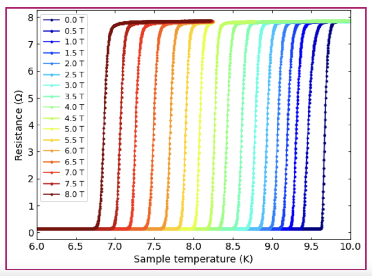
Figure 1: Temperature-dependent resistivity of a NbTi superconductor measured in TeslatronPT
Ben Yager is a senior measurement scientist at Oxford Instruments NanoScience. After completing his PhD, he spent several years as a postdoc at the London Low Temperature Laboratory in the Physics Department of Royal Holloway, University of London, where he studied quantum fluids in confined geometries at temperatures down to 100 microkelvin. He specialised in SQUID detection techniques, especially for nuclear magnetic resonance and thermometry. He subsequently moved to the Institute for Quantum Computing at University of Waterloo, Ontario extending his studies into ultra-sensitive NMR detection where he worked on nano-MRI using force detected NMR.
Abi Graham is a measurement scientist at Oxford Instruments NanoScience. She recently completed her PhD in condensed matter physics at the University of Warwick, where she studied the electronic structure of two-dimensional materials and devices. She focused primarily on twisted heterostructures composed of various combinations of graphene and the semiconducting transition metal dichalcogenides. These heterostructures were characterised predominately using angle-resolved photoemission spectroscopy (ARPES) with in-situ gating at synchrotron facilities such as Diamond Light Source (Oxford, UK) and Electra (Trieste, Italy).

Ben Yager
Senior Measurement Scientist

Abi Graham
Measurement Scientist

© Oxford Instruments 2025